Fills blind vias of various diameters and aspect ratios with excellent fill profile, thin surface copper and minimal dimple — for HDI, flex and silicon substrates.
Key Features
Fills blind vias of various diameters and aspect ratios; fills multiple hole types (blind and through).
Excellent fill profile: thin surface copper, minimal dimple, flat surface.
Short plating time, high productivity.
Stable, durable bath and additive system with high utilization.
Applies to multiple substrate materials (HDI, flex, silicon).
Performance / Application Notes
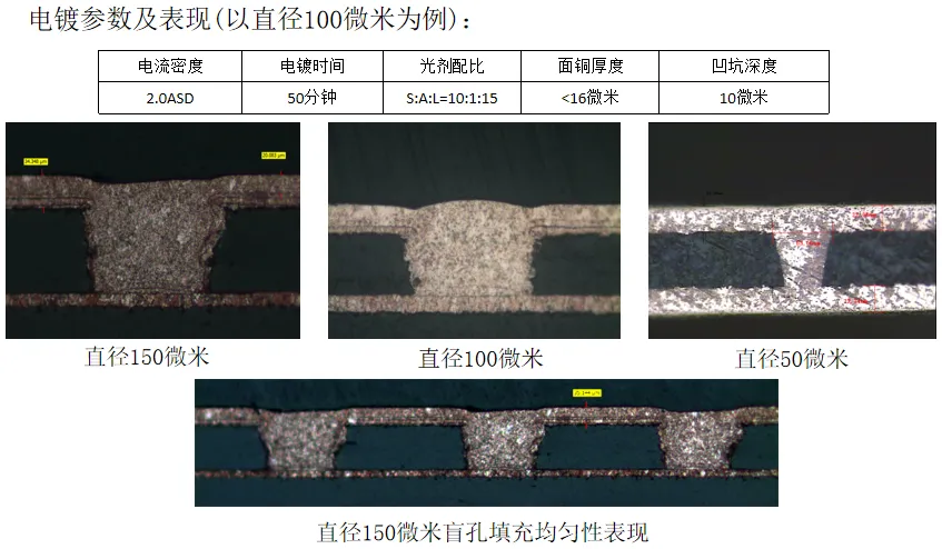
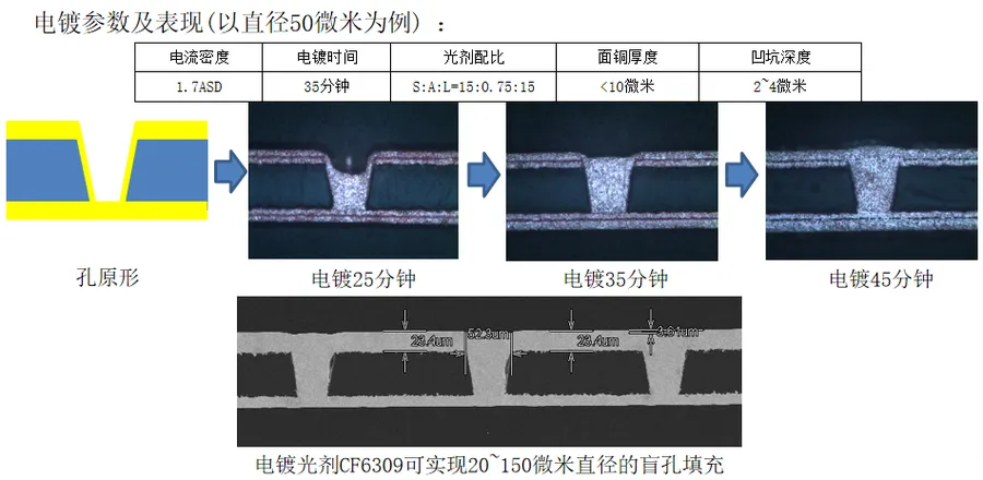
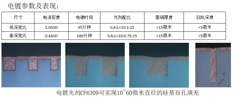
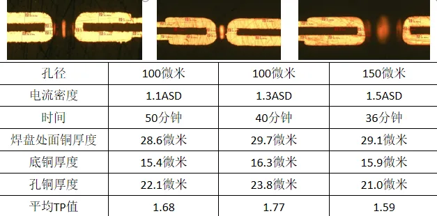
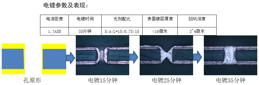
Plating parameters and results (100 μm diameter example): current density 2.0 ASD, plating time 50 min, additive ratio S:A:I = 10:1:15, surface copper < 16 μm, dimple depth 10 μm; blind-via filling at 150/100/50 μm and filling uniformity at 150 μm.Plating parameters and results (50 μm diameter example): current density 1.7 ASD, plating time 35 min, additive ratio S:A:L = 15:0.75:15, surface copper < 10 μm, dimple depth 2–4 μm; the via fills progressively at 25, 35 and 45 min. Additive CF6309 enables blind-via filling for 20–150 μm diameters.Plating parameters (low aspect ratio 2.0 ASD / 45 min; high aspect ratio 0.4 ASD / 180 min; additive ratios S:A:L = 10:1:15 and 10:0.75:15): additive CF6309 enables silicon blind-via filling for 10–60 μm diameters.Flex through-hole plating results: hole diameters 100/100/150 μm, current density 1.1/1.3/1.5 ASD, plating time 50/40/36 min, hole copper 22.1/23.8/21.0 μm, average TP value 1.68/1.77/1.59.Through-hole filling process: current density 1.7 ASD, plating time 35 min, additive ratio S:A:L = 15:0.75:15, surface plating thickness < 10 μm, dimple depth 2–4 μm; the hole fills progressively at 15, 25 and 35 min.